[Courtesy of IBS]
Silicon in a single-crystalline form is commonly used as the main material for semiconductor substrates (wafers) because it is one of the most common elements. It is also very easy to manufacture and manipulate. However, silicon-based semiconductor manufacturing has reached its technological limit, making it harder for wafer producers to further increase the performance of chips.
Transition metal dichalcogenides (TMDs) have high physical and electrical performance characteristics as a two-dimensional substrate material for semiconductors. The mass production of large-scale high-performance single-crystal TMDs faces a technical challenge.
The Institute for Basic Science (IBS) said in a statement on November 16 that a research team led by Professor Feng Ding from the Center for Multidimensional Carbon Materials (CMCM) collaborated with researchers from Peking University (PKU), Beijing Institute of Technology, and Fudan University, to find mechanisms that affect TMDs to grow into a large-sized single-crystal structure.
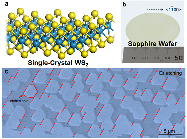
Through demonstrations, the researchers were able to create two-inch-sized single-crystal monofilms using tungsten disulfide (WS2). They also grew single-crystal molybdenum disulfide (MoS2), molybdenum diselenide (MoSe2) and tungsten diselenide (WSe2) on wafer-scale. Researchers proposed a mechanism of "dual-coupling-guided epitaxy growth" for the experimental design of single-crystal TMDs to ensure that all single-crystal grown on a substrate are uniformly aligned.
"This new dual-coupling epitaxy growth mechanism is new for controllable materials growth. In principle, it allows us to realize to grow all 2D materials into large-area single crystals" if proper substrates are available, Ting Cheng, a member of the joint research team, was quoted as saying.
Copyright ⓒ Aju Press All rights reserved.


