SEOUL, January 05 (AJP) - In the premium AI chip race, supremacy is increasingly defined not by transistor density but by advanced packaging — the ability to assemble multiple high-performance chips into a single accelerator capable of handling massive workloads efficiently.
Packaging was once regarded as a back-end step, sealing finished chips into protective casings and mounting them onto boards, work largely handled by outsourced assembly and test firms.
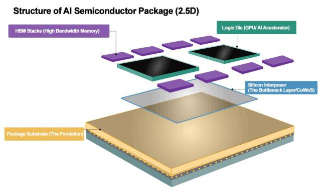
In the era of AI accelerators, however, “advanced packaging” has emerged as a decisive stage of chipmaking, bringing graphics processing units (GPUs) and high-bandwidth memory (HBM) into ultra-close proximity to boost performance, reduce power consumption and shorten time to market.
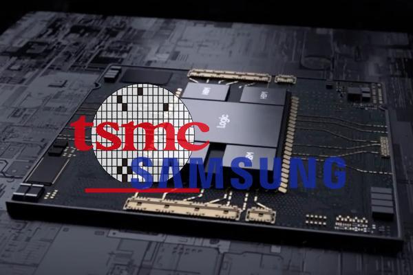
This shift is blurring traditional boundaries between foundries and packaging specialists — and turning packaging capacity into the tightest choke point in the AI supply chain.
“Advanced packaging has become essential — not optional — in the AI era. Without it, AI semiconductors simply cannot be built,” said Ahn Ki-hyun, secretary general of the Korea Semiconductor Industry Association. “Globally, only two companies — TSMC and Samsung — currently possess truly advanced AI packaging capabilities.”
The most sought-after advanced packaging technology today is CoWoS, short for Chips-on-Wafer-on-Substrate, developed by TSMC. The technology allows logic chips and memory stacks to be integrated on a shared substrate, a configuration essential for high-end AI accelerators.
TSMC is struggling to keep up with surging demand from customers such as Nvidia, AMD and major cloud service providers. Google has reportedly scaled back its tensor processing unit (TPU) output target this year despite strong demand, as a significant portion of Taiwan’s CoWoS capacity through 2027 has been reserved for Nvidia — underscoring how critical access to packaging has become.
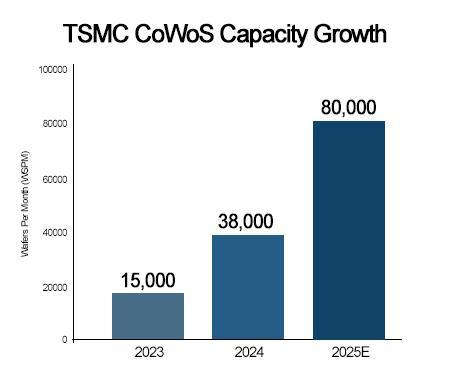
According to TrendForce, TSMC’s monthly CoWoS capacity grew from roughly 13,000–15,000 wafers at the end of 2023 to 35,000–40,000 wafers by late 2024 that doubled to 75,000–80,000 wafers by the end of 2025. The capacity is expected to expand to 120,000 wafers or more in 2026. Even so, demand continues to outstrip supply.
The imbalance has made advanced packaging the most acute bottleneck in AI chipmaking. A single 12-inch wafer typically yields only nine to 10 Nvidia H100-class chips even under near-perfect packaging yields, sharply limiting how quickly AI accelerators can reach the market.
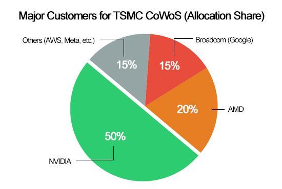
Nvidia is estimated to account for nearly half of TSMC’s CoWoS output, followed by AMD and Broadcom — which manufactures Google’s TPUs. Remaining capacity is shared among customers including Amazon Web Services, Meta and Marvell.
Global shipments of high-end AI accelerators rose sharply in 2024 and are expected to climb further in 2025, intensifying competition for limited packaging slots. Supply constraints have already forced adjustments across the industry, with Google carrying over part of its planned TPU output and server makers such as Dell and Supermicro facing delivery delays that at times stretched beyond 50 weeks.
The ripple effects extend beyond AI chips themselves. Prices for legacy memory such as DDR4 have jumped as manufacturers prioritize high-end AI memory, highlighting the strategic value of tightly integrated memory and packaging capabilities.
Samsung’s opening
The persistent bottleneck is prompting major customers to seek alternatives to TSMC’s near-dominance in advanced packaging — a shift that is bringing Samsung Electronics back into focus.
Unlike most competitors, Samsung can offer a turnkey solution that combines foundry manufacturing, HBM supply and advanced packaging under one roof.
“Samsung holds an integrated edge,” Ahn said. “It has HBM technology, advanced manufacturing capabilities, fabs, and the ability to package HBM together with CPUs or GPUs. If customers bring a design, Samsung can deliver a fully packaged chip.”
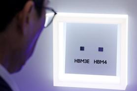
The company’s I-Cube (2.5D) and H-Cube (3D) platforms are designed to integrate logic chips with next-generation HBM, a capability expected to grow more important as the industry moves toward custom memory designs and the HBM4 era.
Samsung’s share of the combined foundry and advanced packaging market remains modest compared with TSMC, but analysts note that the gap itself underscores Samsung’s potential upside as customers pursue multi-vendor strategies to reduce supply-chain risk.
“TSMC, by contrast, does not produce HBM, making it difficult to describe its offering as a full turnkey solution,” Ahn added.
That strategy has begun to yield results. Samsung’s recent win to manufacture Tesla’s AI6 chip, valued at an estimated $16.5 billion, is widely seen in the industry as validation of its integrated approach.
Packaging sets the pace
The growing focus on packaging reflects a broader shift in how AI hardware competitiveness is measured. Even with sufficient GPU designs and memory supply, AI accelerators cannot be shipped without access to advanced packaging lines — making CoWoS and its alternatives the final gatekeeper of AI infrastructure expansion.
As AI workloads scale and next-generation chips such as Nvidia’s Blackwell platform enter the market, the industry’s center of gravity is moving from transistor scaling to assembly capacity. For Samsung, the persistent packaging crunch represents less a threat than a strategic opening — one that could reshape competitive dynamics as customers increasingly prioritize supply-chain resilience over single-vendor dependence.
“From the perspective of Big Tech firms, receiving a completed AI chip from a single provider is highly attractive,” Ahn said. “Given that TSMC cannot absorb all demand on its own, it is increasingly likely that orders will flow toward Samsung.”

Copyright ⓒ Aju Press All rights reserved.