SEOUL, April 27 (AJP) - The traditional line between memory makers and foundries is rapidly blurring as Samsung Electronics and SK hynix pivot toward customized chip production to meet surging artificial intelligence demand.
As AI workloads grow more specialized, Big Tech clients are no longer buying standardized memory at scale but demanding tightly integrated, tailor-made solutions such as High Bandwidth Memory (HBM) co-designed with their own architectures — forcing Korea’s two largest chipmakers to rethink their traditional mass-production model.
Companies like Nvidia and Tesla are driving this shift, pushing suppliers to align memory, logic and packaging into unified, customized stacks. In response, SK hynix and Samsung are increasingly operating less like commodity fabs and more like contract foundries for a handful of deep-pocketed clients.
SK hynix has effectively become a dedicated memory partner to Nvidia, dominating supply of HBM3 and HBM3E used in the latter’s AI accelerators.
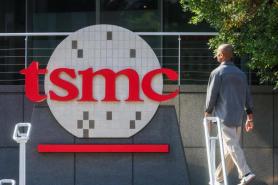
To extend that lead into next-generation HBM4, SK hynix has forged closer ties with TSMC, outsourcing logic foundry work for base dies to leverage TSMC’s 12-nanometer and upcoming 3-nanometer processes.
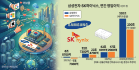
The strategy marks a departure from traditional vertically integrated expansion. Instead of pouring capital into logic fabrication, SK hynix is channeling its estimated 40 trillion won ($29 billion) 2026 capital expenditure into advanced packaging and custom HBM design — prioritizing speed, yield stability and alignment with Nvidia’s roadmap.
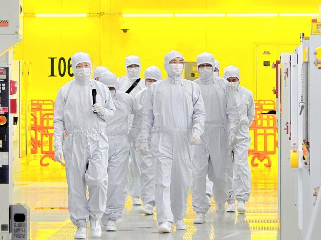
Samsung, by contrast, is leaning into its identity as a full-stack Integrated Device Manufacturer (IDM), combining memory, foundry and advanced packaging under one roof.
It is pitching a “turnkey” model to clients seeking to bypass Nvidia’s ecosystem and build proprietary AI chips. Alongside supplying HBM and foundry services to AMD, Samsung is expanding cooperation with Tesla on next-generation self-driving chips (HW 5.0) and custom memory, while working with AI chip startups such as Tenstorrent and Naver.
To support the shift, Samsung plans to invest about 40.9 trillion won in its Device Solutions division this year, aiming to more than triple its custom HBM capacity.
Industry experts say the transition from standardized memory production to client-specific design will define the next phase of the AI supercycle.
“The market so far has been dictated by the Nvidia–TSMC–SK hynix axis because Nvidia required specific memory components for its GPUs,” said Kim Duk-ki, a professor of semiconductor engineering at Sejong University.
“But as other Big Tech players like Tesla and Intel demand entirely new AI architectures, foundry demand is surging.”
Kim added that while the current AI boom could run for another two years before facing structural constraints such as data center energy limits, Samsung’s breadth offers a strategic hedge.
“Samsung is crucial because it has everything — from memory to foundry,” he said. “Its ability to shift capacity across DRAM, NAND and custom foundry services positions it to adapt to a future where Big Tech dictates increasingly diverse, bespoke chip designs.”

Copyright ⓒ Aju Press All rights reserved.