SEOUL, June 18 (AJP) - SK hynix and Samsung Electronics are locking horns to seize an early lead in next-generation AI memory by shipping samples of their 12-layer HBM4E chips to major customers such as Nvidia for future data-center GPUs including Rubin Ultra.
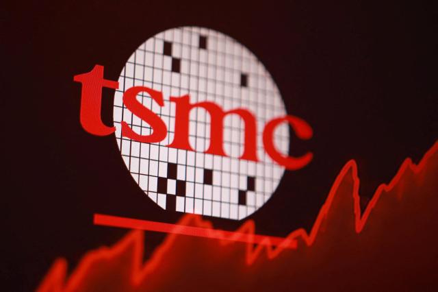
But as the race moves beyond raw memory performance, industry watchers say the real bottleneck may lie elsewhere: Taiwan Semiconductor Manufacturing Co.'s advanced packaging capacity.
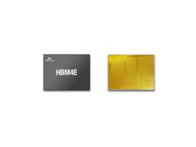
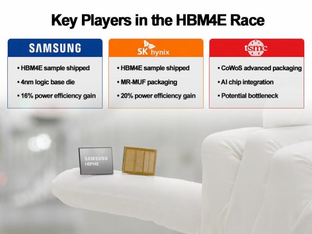
SK hynix said Wednesday it had shipped samples of its 12-layer HBM4E chips to major customers. The new product supports speeds of up to 16 gigabits per second per pin and improves power efficiency by more than 20 percent from the previous generation, according to the company.
The Korean chipmaker is Nvidia's primary HBM supplier for AI accelerators.
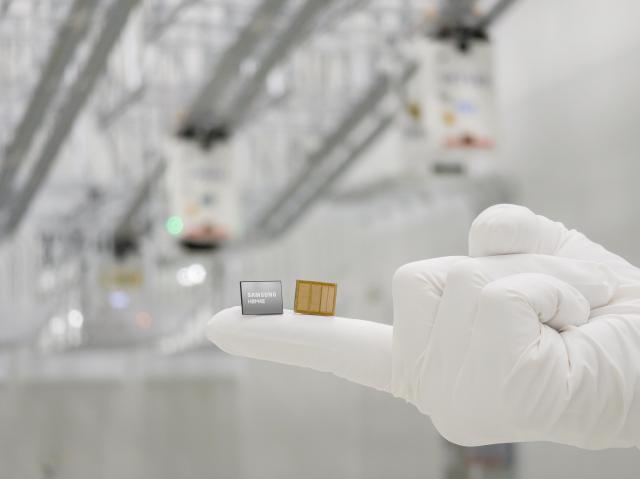
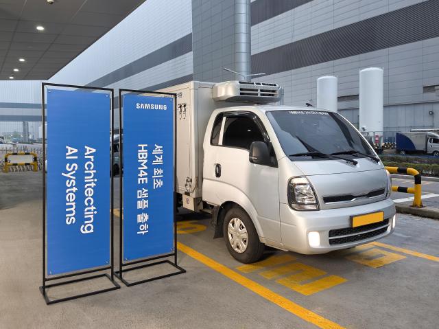
Samsung moved first in late May, announcing shipments of what it called the industry's first 12-layer HBM4E samples to major global customers. Samsung said its chip offers a stable speed of 14Gbps per pin, can scale up to 16Gbps and delivers memory bandwidth of up to 3.6 terabytes per second per stack.
On the surface, the race looks like another chapter in the long-running HBM battle between SK hynix, the current front-runner in AI memory, and Samsung, which is trying to regain ground through more aggressive product launches.
But HBM4E is not simply another faster memory chip.
It is arriving at a point where AI chip performance increasingly depends on how tightly memory, logic chips and packaging technologies are integrated into a single system.
That shift could turn TSMC's CoWoS, or chip-on-wafer-on-substrate technology, into one of the most decisive variables of the HBM4E era.
CoWoS is used to place AI processors and HBM stacks in close proximity, allowing massive volumes of data to move with lower latency and higher bandwidth.
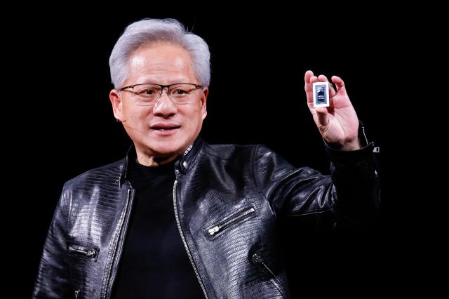
Nvidia Chief Executive Officer Jensen Huang said earlier this year that packaging constraints, though improved from the past two years, remain a bottleneck. Nvidia's Blackwell chips use TSMC's CoWoS-L technology, while Hopper chips continue to rely on CoWoS-S.
That matters for Korean memory makers because HBM qualification is no longer a simple test of whether a memory stack functions on its own.
The chip must perform inside a customer's entire AI accelerator system, where heat dissipation, power efficiency, base-die design and packaging stability can determine whether a product wins final approval.
"Even if the two companies supply products, customers will have to test how they perform when connected with the base die and GPU, including whether heat is managed properly," said Kim Duk-ki, a professor of semiconductor systems engineering at Sejong University.
"The two companies take somewhat different approaches, so performance could differ once the chips are actually connected to GPUs and tested in real applications."
Kim said the final verdict will likely come from customers' own system-level evaluations rather than memory specifications alone.
"As semiconductor technology becomes more customized for each customer, it is difficult for memory suppliers alone to know how the final performance will turn out," he said. "The customer will have to evaluate the products across its own applications."
The customer names have not been disclosed. SK hynix and Samsung have only said they supplied samples to major or global customers.
Still, industry attention is centered on AI chipmakers such as Nvidia, AMD and custom AI chip designers, whose next-generation platforms are expected to drive HBM4 and HBM4E demand.
The packaging issue could complicate the competitive map.
SK hynix has built its lead through close ties with Nvidia and strong execution in HBM3E. Samsung, meanwhile, is emphasizing its ability to combine memory, foundry and packaging technologies, including its use of a 4-nanometer logic base die for HBM4E.
That turnkey strategy could become more valuable if TSMC's capacity remains tight.
But whether Samsung can translate that structural advantage into customer qualification wins remains uncertain. Nor is it clear which supplier will secure the largest allocations for future AI platforms.
Professor Kim said TSMC's packaging capacity could emerge as the industry's biggest constraint, even as HBM supply itself remains tight.
"TSMC is almost dominant globally in CoWoS technology, so it could become a bottleneck," he said. "If that happens, TSMC could gain more pricing power."
The HBM4E race, therefore, may not be decided by who shipped samples first.
Samsung may have claimed the early-mover title, while SK hynix followed within weeks with its own shipments. But the more important milestones are still ahead: customer qualification, packaging integration and mass-production readiness.
For Korea's two largest memory makers, the fight is no longer simply about stacking more DRAM dies faster.
In the AI era, the winner may be the company whose memory not only performs best, but also survives the industry's most unforgiving bottleneck: fitting seamlessly into the world's most advanced AI systems — and securing a place inside TSMC's packaging lines.

Copyright ⓒ Aju Press All rights reserved.