
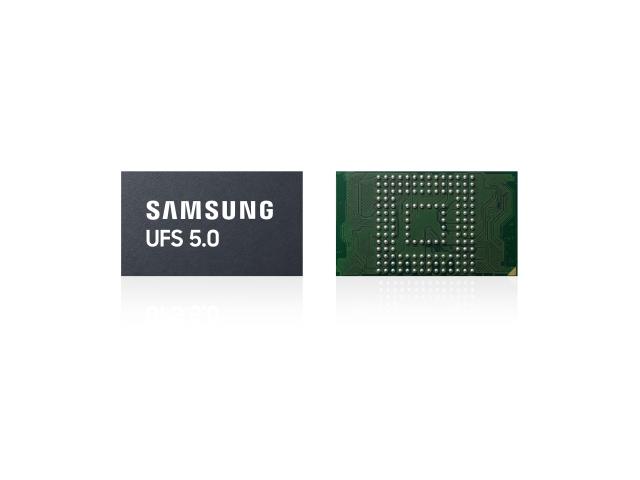
Samsung Electronics UFS 5.0 product
Samsung Electronics has developed the industry's first next-generation mobile memory optimized for on-device artificial intelligence (AI), which operates without network connectivity.
According to Samsung, the new UFS 5.0 memory, designed for use in smartphones and various mobile devices, boasts the highest performance in the industry. Mass production is set to begin in the fourth quarter of this year.
UFS, or Universal Flash Storage, serves as a high-performance embedded flash memory that not only acts as a data storage device but also facilitates the rapid transfer of AI models and large datasets to RAM, enabling application processors (AP) to perform AI computations.
For on-device AI devices that require processing vast amounts of data, semiconductors like UFS are essential.
The newly developed UFS 5.0 memory features both fast data transfer and improved power efficiency.
Built on Samsung's advanced 9th generation V-NAND (V9), it achieves an industry-leading data transfer bandwidth of 10.8 gigabytes per second (GB/s), more than doubling the speed of the previous UFS 4.1. This means it can store and process large data files, such as high-definition 4K and 8K movies, much more quickly.
Power efficiency has also seen significant enhancements. UFS 5.0 incorporates technologies such as clock gating, which disables unused circuits, and multi-voltage technology, which applies optimal voltage to each circuit. As a result, power efficiency has improved by over 40% compared to its predecessor. This reduction in power consumption during data transfer extends the battery life of mobile devices.
The product's size has also been reduced. Samsung has created a package measuring 7.5mm wide, 13mm long, and 0.9mm high, reducing the area by approximately 16.7% compared to the previous model. This compact design enhances flexibility in the design of various form factors, including smartphones, smartwatches, AI wearables, and extended reality (XR) devices, with a maximum capacity of up to 1 terabyte (TB).
Additionally, this product applies the latest UFS 5.0 interface standard from the Joint Electron Device Engineering Council (JEDEC) for embedded flash memory.
Choi Jang-seok, senior vice president of Samsung Electronics' Memory Business Planning Team, stated, "In the era of on-device AI, storage devices are becoming a key factor that determines the AI experience, beyond just being data storage spaces. With the completion of the industry-first UFS 5.0 development, Samsung will continue to set new standards for next-generation mobile storage and lead AI mobile innovation."
According to Samsung, the new UFS 5.0 memory, designed for use in smartphones and various mobile devices, boasts the highest performance in the industry. Mass production is set to begin in the fourth quarter of this year.
UFS, or Universal Flash Storage, serves as a high-performance embedded flash memory that not only acts as a data storage device but also facilitates the rapid transfer of AI models and large datasets to RAM, enabling application processors (AP) to perform AI computations.
For on-device AI devices that require processing vast amounts of data, semiconductors like UFS are essential.
The newly developed UFS 5.0 memory features both fast data transfer and improved power efficiency.
Built on Samsung's advanced 9th generation V-NAND (V9), it achieves an industry-leading data transfer bandwidth of 10.8 gigabytes per second (GB/s), more than doubling the speed of the previous UFS 4.1. This means it can store and process large data files, such as high-definition 4K and 8K movies, much more quickly.
Power efficiency has also seen significant enhancements. UFS 5.0 incorporates technologies such as clock gating, which disables unused circuits, and multi-voltage technology, which applies optimal voltage to each circuit. As a result, power efficiency has improved by over 40% compared to its predecessor. This reduction in power consumption during data transfer extends the battery life of mobile devices.
The product's size has also been reduced. Samsung has created a package measuring 7.5mm wide, 13mm long, and 0.9mm high, reducing the area by approximately 16.7% compared to the previous model. This compact design enhances flexibility in the design of various form factors, including smartphones, smartwatches, AI wearables, and extended reality (XR) devices, with a maximum capacity of up to 1 terabyte (TB).
Additionally, this product applies the latest UFS 5.0 interface standard from the Joint Electron Device Engineering Council (JEDEC) for embedded flash memory.
Choi Jang-seok, senior vice president of Samsung Electronics' Memory Business Planning Team, stated, "In the era of on-device AI, storage devices are becoming a key factor that determines the AI experience, beyond just being data storage spaces. With the completion of the industry-first UFS 5.0 development, Samsung will continue to set new standards for next-generation mobile storage and lead AI mobile innovation."
* This article has been translated by AI.
Copyright ⓒ Aju Press All rights reserved.