
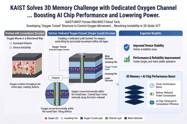
SEOUL, August 20 (AJP) - In a bid to stabilize memory stacked directly on top of artificial intelligence chips, a joint research team led by the Korea Advanced Institute of Science and Technology said Thursday it had developed an insulating film that steers oxygen atoms toward the parts of a vertical memory transistor that need them and away from the parts they damage, allowing the devices to achieve higher current flow and longer data retention.
The device held its electrical characteristics after more than 10 million switching cycles, with the voltage at which the transistor switches on drifting by less than 50 millivolts. A test memory cell built around it held stored data for more than 648 seconds, close to 11 minutes, without being refreshed, and survived more than 1,200 write cycles.
The biggest drain on an AI chip is not the arithmetic. It is the constant shuttling of data between the memory that stores it and the processor that computes on it. Stacking the two together is one of the few remaining ways to shorten that trip, and oxygen has been the specific thing breaking it.
For decades the memory industry improved chips by making each component smaller, packing more storage into the same square of silicon while drawing less power. That approach is now close to its physical floor.
The alternative is to build upward, stacking components in three dimensions rather than shrinking them sideways. It is what a city does when it runs out of room for single-story houses and starts putting up apartment towers.
The vertical channel transistor is one way to do that. In a conventional transistor, current runs horizontally through a strip of material called the channel. Turning that channel on its end frees floor space, letting engineers pack far more devices into the same area.
Making the channel out of an oxide semiconductor rather than silicon adds a second advantage. Oxide leaks very little current when switched off, which is what allows a memory cell to hold its contents without constant electrical topping up.
The trouble is oxygen.
Oxide channels are missing some of the oxygen atoms that belong in their crystal structure, a defect known as an oxygen vacancy. A few of them help current flow. Too many and the transistor stops behaving predictably.
The obvious remedy is to feed oxygen back into the channel. But oxygen does not stay where it is put. It migrates to the metal electrodes and corrodes them, raising resistance and degrading the device that the repair was meant to improve.
The Korea Advanced Institute of Science and Technology (KAIST) team attacked the problem through the interlayer dielectric, the insulating film that separates the wiring and components inside a chip. Engineers normally treat it as an electrical barrier and nothing more.
By sandwiching silicon dioxide between two layers of silicon nitride, the researchers turned the film into what they call an oxygen tunnel. It is a one-way passage that lets oxygen reach the channel where it is needed and blocks the path toward the electrodes where it does damage.
KAIST said the resulting transistors achieved the highest current flow and data retention reported for oxide vertical channel devices.
The team then combined the oxide transistors with conventional silicon CMOS circuitry, the basic technology inside almost every processor and phone chip made today, and modeled how the hybrid would perform as embedded memory. Simulations projected roughly 45 times longer data retention than a comparable CMOS design and a 38 percent smaller memory cell.
The payoff the researchers are aiming at is compute-in-memory, an approach that performs calculations inside or beside the memory that holds the data instead of hauling that data across the chip to a separate processor.
The current arrangement is the equivalent of carrying every ingredient from the pantry to a kitchen in another building and back again. As AI models grow, the carrying costs more energy than the cooking.
Kwon Ji-min, a professor in KAIST's School of Electrical Engineering, led the work.
"Building a tall building is not just about adding floors, it is about making the structure stable, and the same is true of three-dimensional semiconductors," Kwon said. "This technology should speed up development of next-generation memory that raises AI processing speed while cutting power consumption."
Gu Hyeon-ho was the first author. Lee Yong-woo and Jung Hak-soon were co-corresponding authors with Kwon.
Researchers from the Ulsan National Institute of Science and Technology, Yonsei University, the Korea Research Institute of Chemical Technology, Seoul National University of Science and Technology and Seoul National University also took part.
Several claims remain untested outside the laboratory. The results were demonstrated on individual transistors and a small test memory cell, not on a production wafer. The 45-fold retention gain and the 38 percent area saving are simulation outputs rather than measurements from fabricated hardware.
No full compute-in-memory array using the design has been built, and KAIST did not name a manufacturing partner.
The paper ran in the materials science journal Advanced Functional Materials on May 20 and was selected as a front cover article. KAIST announced the results Thursday, three months after publication.
AJP Takeaways
● A KAIST-led team built a three-layer insulating film that steers oxygen inside a stacked memory transistor, removing the defect problem that has blocked 3D memory for AI chips.
● The device held steady after more than 10 million switching cycles, with switch-on voltage drifting under 50 millivolts. A test memory cell retained data for more than 648 seconds without a refresh.
● Simulations pairing the oxide transistors with silicon CMOS projected 45 times longer data retention and a 38 percent smaller memory cell than a comparable conventional design.
● Those projections have not been verified in fabricated hardware, and no full compute-in-memory array has been built.

Copyright ⓒ Aju Press All rights reserved.