SEOUL, October 14 (AJP) - Shares of the world’s leading memory makers have nosedived this week on heavy selling after China’s ChangXin Memory Technologies (CXMT) stepped up its catch-up push by targeting the server memory market.
Samsung Electronics, the leader of the three-way memory oligopoly it has long shared with SK hynix and Micron, put a sweeping lineup on display at SEDEX 2026 in Seoul, from HBM4E to advanced packaging, as if to show it is still pulling ahead.
Under the theme “Architecting AI Systems,” the South Korean tech giant unveiled a broad range of AI semiconductor solutions at SEDEX 2026, which runs at COEX in southern Seoul from Oct. 14 to 16.
The exhibition highlighted Samsung’s ability to combine memory, logic design, foundry manufacturing and advanced packaging. Those capabilities could become more important as AI processors grow more complex and demand faster, more energy-efficient data transfer.
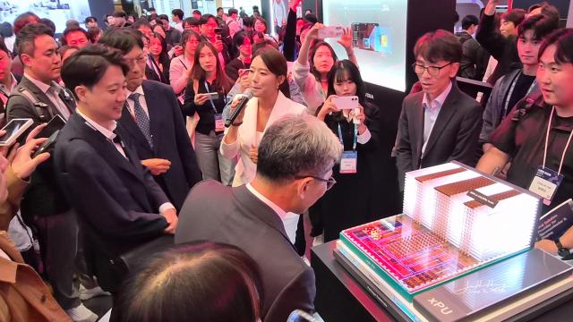
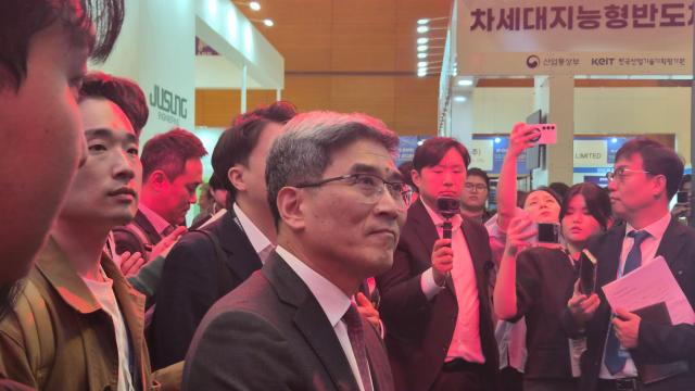
Song Jae-hyuk, chief technology officer of Samsung’s chip division, led a VIP tour of the exhibition. He was joined by lawmaker Lee Jun-seok and Ahn Hyun, president and chief development officer of rival SK hynix.
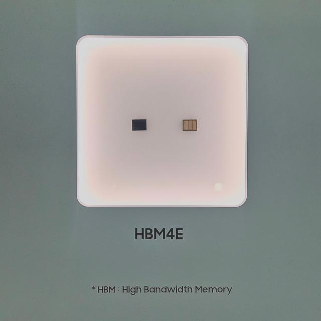
At the center of Samsung’s display was HBM4E, the next generation of high-bandwidth memory designed for increasingly demanding AI workloads.
The company also showcased emerging memory architectures aimed at overcoming the limits of conventional chip designs.
Among them was zHBM, a three-dimensional memory architecture that shortens the physical distance between processors and memory, potentially improving data-transfer efficiency. Samsung displayed a mock-up of the technology alongside zNAND-O, a 3D NAND solution for edge AI applications.
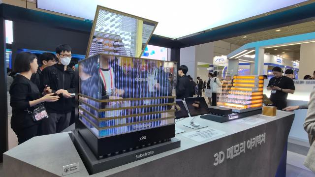
Another exhibit featured LPDDR-PIM, which builds processing capability directly into memory to reduce the need to shuttle data between processors and memory chips.
Samsung’s foundry business demonstrated its role in the AI supply chain with a 4-nanometer HBM4E base die. It also showed advanced packaging technologies that connect multiple chips within a single system.
These included 2.3D Cube-E, a high-density packaging solution based on silicon bridges, and 3D Cube-H, which uses three-dimensional integration.
The company also displayed a 2-nanometer gate-all-around wafer and a model of a co-packaged optics (CPO) interconnect, which converts electrical signals into optical signals for high-speed data transmission.
Together, the technologies underscored Samsung’s strategy of offering customers an integrated semiconductor platform rather than competing solely on the performance of individual memory chips.
Its System LSI division presented a DIMM solution for server memory modules, the 200-megapixel ISOCELL HPC image sensor and the Exynos 2600 mobile processor. Those products extended the showcase beyond data centers to smartphones and other AI-enabled devices.
Separately, Song confirmed to reporters that Samsung is researching 4F² DRAM. The next-generation architecture drew fresh market attention after CXMT said it would launch server memory modules built on the technology by the end of the year.
The technology increases memory density by shrinking the area each DRAM cell occupies, though the economics of mass production remain a key hurdle.
Song did not disclose the progress of Samsung’s research, a rare instance of a Korean chipmaker responding to, rather than leading, a next-generation memory announcement.
Beyond its technology roadmap, Samsung used the exhibition to outline plans for expanding South Korea’s chipmaking base.
The company said it plans to invest about 360 trillion won ($250 billion) in its planned semiconductor complex in Yongin, south of Seoul. Site preparation and construction are scheduled to begin in 2027.
Samsung aims to bring the complex’s first production line online in October 2029.
The complex is expected to house around 70 suppliers of semiconductor materials, components and equipment, as well as fabless chip designers. Together they would form an ecosystem linking manufacturing with research and development.
Samsung also highlighted its supplier support programs. It noted that it received the top rating in South Korea’s 2025 shared growth evaluation for the 14th consecutive year.
SEDEX 2026, organized by the Korea Semiconductor Industry Association, brings together about 300 companies across the semiconductor supply chain, including memory and logic chipmakers, equipment makers and materials suppliers.

Copyright ⓒ Aju Press All rights reserved.