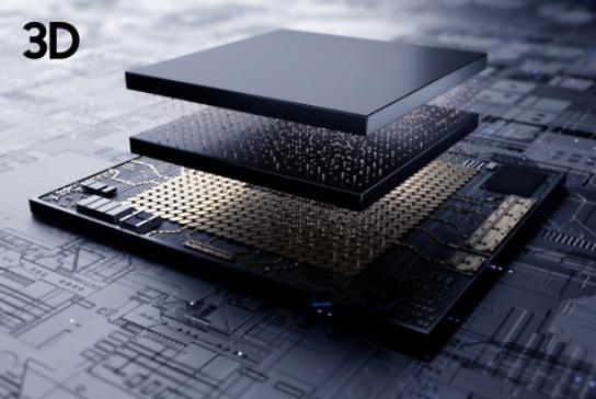
[Courtesy of Samsung Electronics]
SEOUL --For most advanced process nodes, Samsung Electronics applied its silicon-proven 3D IC packaging technology called "X-Cube (eXtended-Cube) that enables significant leaps in speed and power efficiency to help address the rigorous performance demands of next-generation applications.
With X-Cube, chip designers can enjoy greater flexibility to build custom solutions that best suit their unique requirements, Samsung said in a statement, adding that X-Cube's silicon-proven design methodology and flow are available now for advanced nodes including 7nm and 5nm.
"Samsung’s new 3D integration technology ensures reliable TSV (through-silicon via) interconnections even at the cutting-edge EUV (extreme ultraviolet) process nodes," said Kang Moon-soo, senior vice president of Samsung's foundry market strategy, was quoted as saying. "We are committed to bringing more 3D IC innovation that can push the boundaries of semiconductors."
Samsung said it would continue collaborating with global fabless customers to facilitate the deployment of 3D IC solutions in next-generation high-performance applications.
Samsung has revealed a massive investment to strengthen its competitiveness in System LSI and foundry businesses, saying it aims to become the world leader in not only memory semiconductors but also logic chips.
Samsung said on May 21 that it would establish a new production line in Pyeongtaek to focus on 5-nanometer (nm) and below process technology based on EUV for making high-performance semiconductors. EUV chip manufacturing is a technology using extreme ultraviolet light wavelengths to expose an ultra-thin electrical circuit.
Copyright ⓒ Aju Press All rights reserved.


