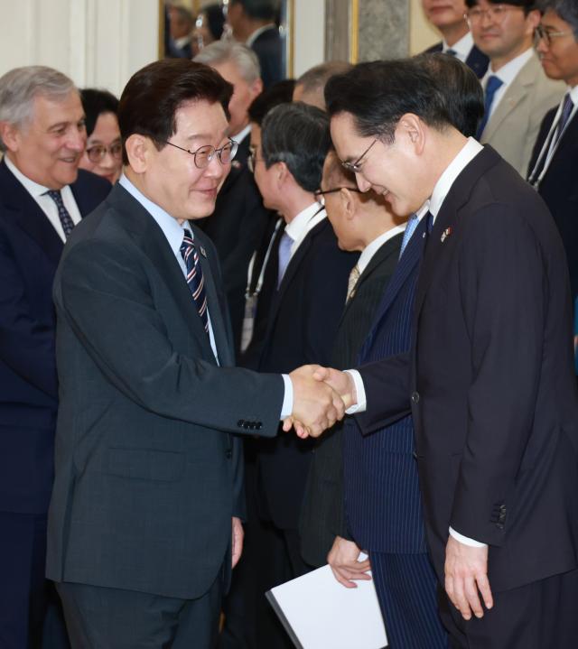
The colossal investment plan — tantamount to nearly half of the country's annual gross domestic product — was outlined during a meeting between President Lee Jae Myung and Samsung Group Chairman Lee Jae-yong on Thursday and will be announced on Monday, when the government unveils its initiative to create the second chipmaking belt in the southern region, according to local reports.
Chipmaking facilities of Samsung Electronics and SK hynix are clustered around the capital region, where further expansion is becoming increasingly difficult due to shortages of land, water and power infrastructure.
The government announcement will include fast-tracked approvals, licensing exemptions and investment incentives.
Under the outline, Samsung Electronics plans to build four to five fabs across the Honam region, including Gwangju and South Jeolla Province, costing around 300 trillion won, as a sub-5-nanometer fab usually costs around 60 trillion won.
Separately, the company is looking to accelerate its project to build six fabs in the nascent Yongin chip cluster by 2048, bringing the schedule forward by at least 10 years.
In the central Chungcheong region, Samsung is expected to establish a new research and manufacturing base for advanced chip packaging and AI datacenters.
The massive investment is likely to be matched by SK Group, amid growing debate over reinvesting the windfall generated by the memory chip boom.
Samsung Electronics and SK hynix together account for nearly 80 percent of the high-bandwidth memory market, supplying the chips that power AI accelerators and hyperscale datacenters.
The investment push reflects an emerging national strategy to channel unprecedented AI-driven semiconductor profits into expanding manufacturing capacity, advanced packaging and AI infrastructure, reinforcing South Korea's position in the global AI supply chain.
Copyright ⓒ Aju Press All rights reserved.