

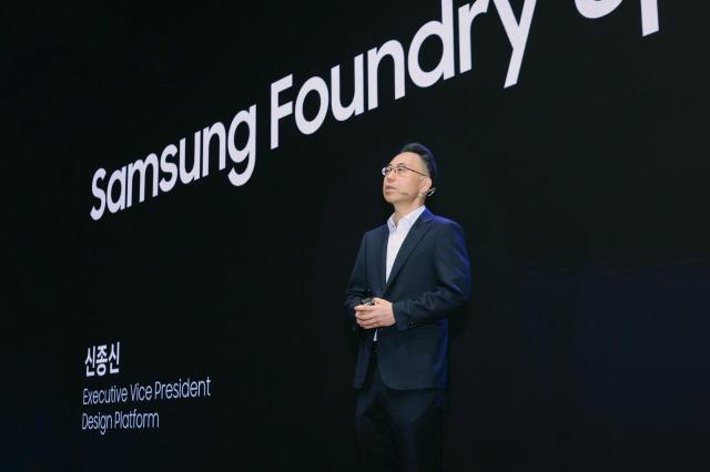
Samsung Electronics unveiled its strategies for collaboration in the artificial intelligence (AI) semiconductor ecosystem and next-generation foundry technologies on July 1, 2026, at its Seocho office in Seoul. The event, themed "Connecting Semiconductor Innovation in the AI Era," attracted over 400 attendees from client and partner companies.
In May, the company held the annual SAFE Forum 2026 for global clients in California.
During his keynote address, Shin Jong-shin, head of Samsung's Foundry Division Design Platform Development, stated, "We will strengthen collaboration with global AI high-performance computing (HPC) clients and domestic system semiconductor companies, expanding our role beyond foundry production to support the domestic system semiconductor industry as a platform."
At the event, 21 partner companies showcased various solutions in areas such as EDA, IP, DSP, VDP, and MDI.
Key partners shared their AI semiconductor development cases. Park Sung-hyun, CEO of Rebellion, presented the development of the 'Rebel100' neural processing unit (NPU) based on Samsung's 4-nanometer process and advanced packaging, hinting at future collaboration for sovereign AI development.
Jin Marie Brunet, Senior Vice President of Siemens EDA, emphasized support across yield, design verification, reliability, and packaging, stating that they would assist in implementing AI and HPC semiconductors through Samsung's advanced processes.
Samsung also presented its AI-customized process roadmap, which aims to maximize chip performance through design technology optimization (DTCO) strategies, high-performance SRAM technology, and next-generation 2-nanometer process technology, thereby enhancing power, performance, and area (PPA) competitiveness to support clients' next-generation product development.
The company plans to expand collaboration with the government and industry to foster the domestic system semiconductor ecosystem. Samsung is participating in the Manufacturing AI Transformation (M.AX) alliance promoted by the Ministry of Trade, Industry and Energy to advance the development of low-power, high-performance on-device AI semiconductors for automotive, home appliances, robotics, and defense applications.
Additionally, Samsung aims to enhance semiconductor R&D through the Multi Project Wafer (MPW) program and the K-Chips initiative, focusing on supporting prototype production and training specialized personnel.
* This article has been translated by AI.
Copyright ⓒ Aju Press All rights reserved.