
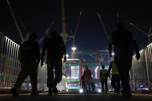
This is the second installment of AJP's Chip Republic series, offering a rare first-hand look inside Samsung Electronics' next-generation fab construction site as the chip giant races to defend its technological supremacy.
PYEONGTAEK, August 10 (AJP) - At 3:45 a.m., with the worst of the day's heat still hours away, Samsung Electronics' race to build its next great semiconductor factory is already underway.
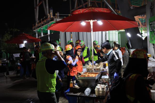
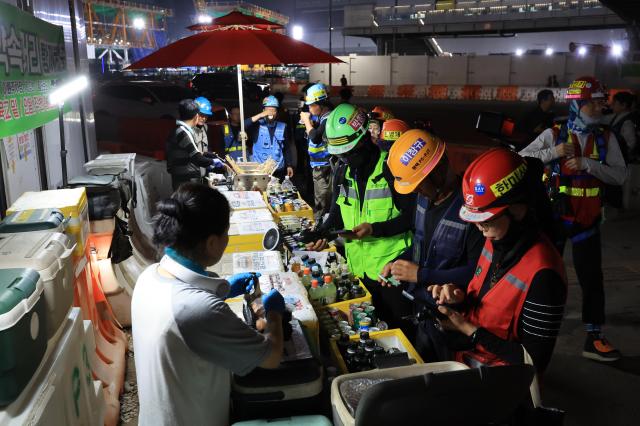
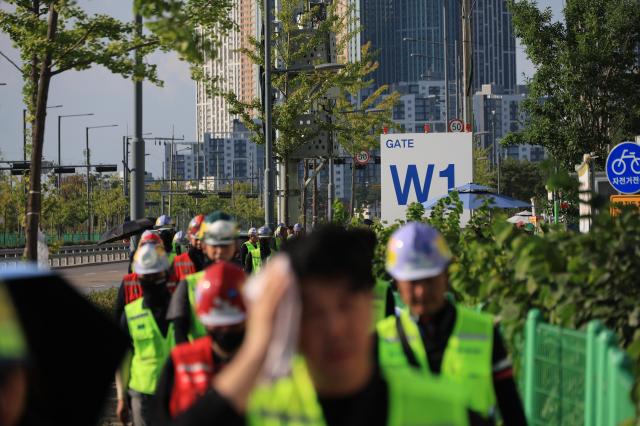
Temporary food stalls appear in the darkness outside P5, the giant new fab rising inside Samsung's flagship Pyeongtaek chip complex.
Steam curls from pots of fish cakes and tteokbokki as workers in hard hats marked with their names and blood types grab rolls of gimbap and coffee before filing through the gates for shifts starting around 5 a.m.
There is little time to waste.
Samsung is advancing construction of P5 toward 2028 from an initial 2030 timetable, accelerating a factory expected to underpin its next generation of advanced memory as artificial intelligence drives an increasingly fierce race for production capacity.
The timetable is tightening just as South Korea's extreme summer heat is squeezing the hours available to build it.
At 35 degrees Celsius in apparent temperature, Samsung C&T stops high-risk work except in limited circumstances. At 38 degrees, outdoor and other heat-sensitive operations are prohibited.
Hwang, 60, joins the stream of workers heading toward P5 before dawn.
"Getting up this early and coming to work every day is still difficult," he said. "And in this heat, I still walk to work."
Park, a subcontracted worker in her 40s who has spent about a year at the site, eats before going inside.
"I eat before going in because once we're inside, we work for a long time," she said.
"These days, especially with the heat, you need to eat properly and manage your condition."
An ambulance stands nearby for workers suffering from fatigue or heat-related symptoms.
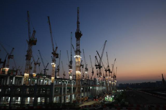
By sunrise, the food stalls have vanished. Workers are behind the gates, trucks are moving and cranes hang over the unfinished fab as the temperature begins its climb.
The scene is the physical underside of the AI boom.
For consumers, artificial intelligence arrives through a screen. In Pyeongtaek, it is arriving in concrete, steel, pipes, cleanrooms and billions of dollars of machinery — all being put in place years before anyone knows exactly how much computing power the world will demand.
A bridge built for wafer traffic
If the dawn shift captures the urgency, a structure taking shape above the campus shows the precision.
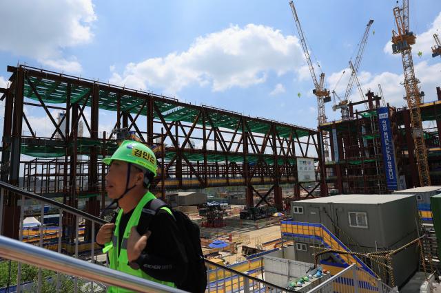
Samsung is building a roughly 360-meter elevated bridge between its existing P4 fab and the future P5. It is not for human travel.
"The structure currently under construction will connect P4 and P5 through an overbridge designed exclusively for moving chips," an official close to the company told AJP.
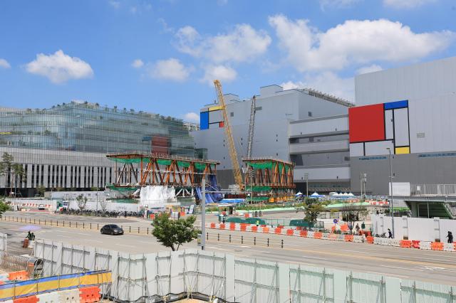
"It is not a passageway for people at all. It is one of the site's most important structures."
The bridge will be about three times as long as a comparable 120-meter structure at Samsung's Hwaseong semiconductor complex.
Wafers will eventually move back and forth across it as different stages of production are carried out in P4 and P5.
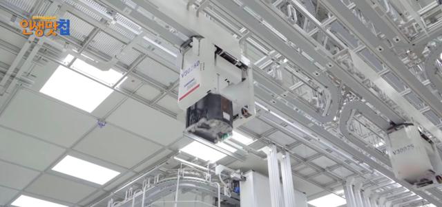
"The bridge is being built so wafers can move back and forth between P4 and P5 as different processes are carried out," the official said.
In an advanced fab, that traffic is part of production.
A wafer leaving one process may need equipment housed elsewhere before moving to the next. Each transfer, queue and bottleneck affects how quickly costly machinery can be used and how smoothly production moves through the line.
The bridge effectively turns P4 and P5 from neighboring factories into parts of one manufacturing system.
Hundreds of meters of overhead wafer traffic may look like infrastructure. In chipmaking, the precision of that flow can define a fab's competitiveness.
Samsung's Pyeongtaek campus already covers about 2.9 million square meters, roughly 1.4 times the territory of Monaco, or around 400 soccer fields, capable of housing six fabs.
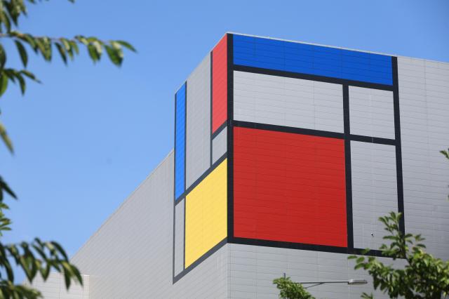
Samsung broke ground on the first Pyeongtaek fab in May 2015 under an initial investment plan of 15.6 trillion won. The final cost rose to around 30 trillion won.
Mass production began in July 2017 with fourth-generation 64-layer V-NAND. Construction on a second line followed in 2018, with advanced DRAM production beginning in 2020.
What started with one giant fab has become Samsung's flagship chipmaking campus.
AI is now setting the pace for its next expansion.
P5, whose cost is estimated at around 60 trillion won, is expected to become a major production base for advanced memory including high-bandwidth memory, or HBM, the stacked chips feeding data to AI accelerators.
But building it is increasingly a race in itself.
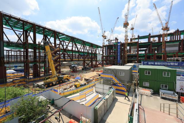
"P5 is different from the projects we have experienced before in terms of both scale and complexity," a Samsung C&T project official overseeing the work told AJP.
"The success of P5 is not simply about meeting a construction schedule and completing a building," the official said, citing the need to maintain safety, quality and productivity while responding quickly to changing conditions.
AI moves into Korea's capital spending
The cranes in Pyeongtaek are beginning to show up in South Korea's investment numbers.
Facility investment rose 13 percent from a year earlier in the second quarter, while investment in machinery climbed 15 percent, according to official industrial-activity data.
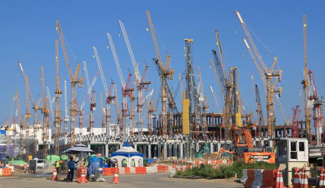
The pace accelerated sharply in June. Facility investment jumped 21.7 percent on year and machinery investment 22.2 percent, with semiconductor-manufacturing equipment among the drivers.
P5 is among the most visible manifestations of that capital cycle.
Rival SK hynix is more than 70 percent through construction of its first fab at the Yongin semiconductor cluster. On Friday, its board approved 35.2 trillion won for a second Yongin fab, known as Y2, and another 19.1 trillion won for the M17 fab in Cheongju.
Together, the two projects amount to roughly 45 percent of SK hynix's shareholders' equity of 120.7 trillion won. The Yongin investment alone represents 29.19 percent.
The spending reflects a basic mismatch in the AI race.
A new generation of AI accelerators can arrive within a year. A semiconductor fab takes years to build, equip and qualify.
By the time demand becomes certain, it can already be too late to build the factory needed to meet it.
Samsung and SK hynix are therefore competing not only over who can develop better memory, but who will have enough cleanroom space and equipment ready when customers want it.
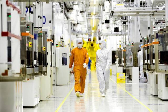
That makes investment itself part of the competition.
"When you invest, you expand your manufacturing facilities and your production scale. That gives you leadership in the market," said Ahn Ki-hyun, executive director of the Korea Semiconductor Industry Association. "If you don't invest while your competitors do, you lose that leadership."
Ahn cautioned, however, against viewing P5 alone as something that would fundamentally shift the balance between Samsung and SK hynix. Both companies are accelerating investment, he said, making the race less about whether to expand than about how quickly each can turn new capacity into products and sales.
The memory boom gets broader
The market is giving them reason to hurry.
The first phase of the AI memory boom centered on HBM, where SK hynix established an early lead and Samsung has been working to catch up through newer generations including HBM4.
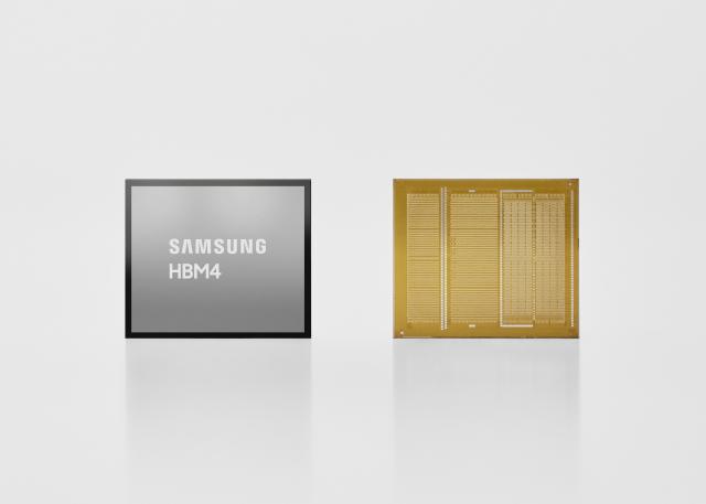
Now the shortage is spreading.
As Samsung, SK hynix and Micron devote more capacity to HBM and other high-value server products, less is available for conventional DRAM. AI servers themselves consume large quantities of DRAM, tightening the market from both sides.
NAND flash is joining the cycle as enterprise solid-state drives absorb the vast stores of data needed by AI systems.
Sigmaintell expects global semiconductor revenue to reach about $1.59 trillion this year, with memory accounting for roughly 60 percent. It sees DRAM revenue rising more than 300 percent and NAND nearly 250 percent, with the HBM market alone topping $100 billion.
Omdia has raised its semiconductor growth forecast to 94.1 percent and likewise expects memory to account for more than half of industry revenue, with bottlenecks in HBM, advanced packaging and leading-edge production persisting into 2027.
Counterpoint Research expects servers to account for 56 percent of memory revenue this year, up from 37 percent last year, another sign that the industry's center of gravity is moving away from consumer electronics.
The firms use different definitions and methodologies, and their headline market estimates are not directly comparable. Their direction is the same: AI is pulling HBM, DRAM and NAND into the same investment cycle.
Samsung and SK hynix are benefiting across that spread.
Samsung held 39 percent of the global DRAM market by revenue in the second quarter, while SK hynix's DRAM revenue more than tripled from a year earlier, according to market estimates.
The boom is also drawing competitors. China's CXMT and Taiwan's Nanya posted explosive revenue growth as the three dominant memory makers concentrated more capacity on premium products.
That is another reason Samsung cannot assume today's shortage will last forever.
Memory has always been cyclical: shortage drives investment, investment creates supply, and supply eventually puts pressure on prices.
AI has not repealed that cycle. It has made waiting for certainty more costly.
The people beneath the cleanroom
Inside P5, the language of artificial intelligence quickly disappears.
Workers erect structures, install partitions, electrical systems and pipes, clean equipment and guide vehicles through the site.
"There are so many people inside that you can't count them," one female worker said after leaving work.
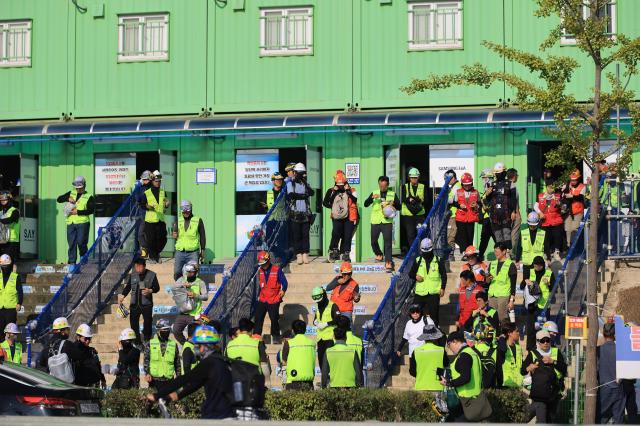
"It's extremely busy inside," another said.
Kim, a subcontracted worker installing partitions around equipment areas, said the sophistication of the technology rarely enters his working day.
"We don't really know whether it's a 2-nanometer process or a 3-nanometer process," he said.
"What we do know is that the equipment is extremely expensive. So we're always told to be careful around it."
"To us, it's construction work," he said. "You do your own job properly and make sure you don't damage anything."
Workers also describe another structure running through P5: a rigid contracting hierarchy.
Samsung Electronics owns the complex. Samsung C&T oversees major construction. Beneath them sit first-tier contractors, subcontractors and smaller specialist crews.
"There's definitely a hierarchy here," said a supervisor who has worked across Samsung's semiconductor sites.
"Samsung Electronics is at the top, then Samsung C&T, then the first-tier contractors, and then companies below them."
Some subcontracted workers jokingly call Samsung Electronics employees "juin-nim," literally "master."
"We call them 'juin-nim,'" one worker said with a laugh. "This place is basically a class society."
Different employers can mean different gates, dining facilities, buses and schedules.
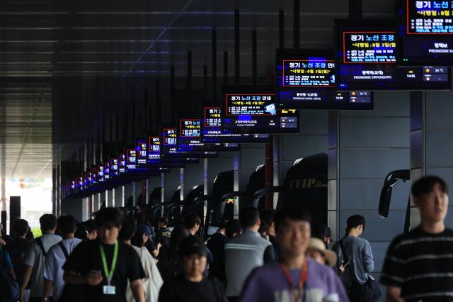
"We don't really mix much with Samsung employees," one worker said. "The gates we use are different, the places we eat can be different, and even the times we use them can be different."
The hierarchy becomes most consequential when work stops.
"If you're with a first-tier contractor like us, missing a day isn't necessarily a huge problem," the supervisor said. "We can move the work to another day."
"But for people working for subcontractors of subcontractors, that day itself is money."
And in the heat, work does stop.
On days when apparent temperatures reach the site's safety thresholds, shifts can end only hours after they begin. The companies can rearrange schedules; workers further down the contracting chain can lose the day's income.
The danger is more immediate than the lost hours.
Workers said ambulances had become a familiar sight.
"Just yesterday, five workers collapsed with heat-related illnesses, and ambulances were going back and forth," one worker said.
The official temperature, however, tells only part of the story.
"The temperature measured by weather authorities is essentially a background atmospheric temperature, taken under open and well-ventilated conditions," said Choi Yong-Sang, a climate scientist at Ewha Womans University. "At an actual work site, conditions can be much hotter."
Asphalt surfaces can exceed 60 degrees Celsius, while concrete, poor ventilation and enclosed spaces can further raise workers' thermal exposure, Choi said. Heavy protective clothing, helmets and crowded working conditions add another layer of risk.
"You cannot control the outside temperature," Choi said. "So to reduce heat stress, you have to reduce workers' exposure or vulnerability."
P5 will be built. The question is how fast.
Samsung has pulled its timetable forward to 2028 from 2030. On the ground, the working day is being pulled forward too, toward the cooler hours before sunrise.
Above the site, the unfinished wafer bridge reaches toward P5. Below it, cranes, trucks and thousands of workers race a clock that can stop by late morning when the heat becomes too much.
One day, wafers carrying Samsung's most advanced memory will cross that bridge on their way into AI machines around the world.
For now, the traffic is human.
At 3:45 a.m. tomorrow, it starts again.

Copyright ⓒ Aju Press All rights reserved.