
SEOUL, October 28 (AJP) - A Kookmin University engineer who works on stacking chip layers without damaging the layers below them has been named among the world's most-cited researchers for the sixth consecutive year.
Choi Sung-jin, a professor in the university's Department of Electronics Engineering, appeared on both lists of the 2026 "World's Top 2% Scientists" ranking compiled by Stanford University and Elsevier, the Dutch academic publisher. In applied physics, he placed in roughly the top 1.3 percent by career-long impact and the top 0.9 percent for the most recent single year.
The ranking draws on Elsevier's Scopus database, which tracks how often academic papers are cited, and scores researchers against others in the same field. One list covers a researcher's entire career, while the other measures citation impact over a single year. Choi has been on the list every year since 2021.
Google Scholar counts more than 25,000 citations of his work and gives him an h-index above 70. That means at least 70 of his papers have each been cited 70 times or more.
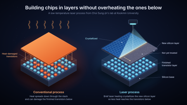
Choi's research targets a basic limit in chipmaking. Engineers pack more computing power into a chip by building transistors in vertical layers, known as 3D integration. Forming each new layer usually takes high heat, which can damage the finished layer underneath.
His team developed a low-temperature process that uses a laser to heat silicon for a very short time and crystallize it. The team then used the method to build nanosheet transistors, which are made from very thin layers of silicon. Kookmin described the approach as a foundation for dense logic and memory chips, because new devices can be formed on top while less heat reaches the ones below.
Choi also works with carbon nanotubes, which are tiny cylinders of carbon atoms that conduct electricity and are studied as a material for future transistors. His group analyzed large numbers of nanotube transistors made on 8-inch wafers, the discs on which chips are produced. By combining experiments with computer simulations, the team identified how device size and the way the nanotubes connect affect performance.
More recently, he has moved into artificial intelligence and hardware security. One project builds carbon nanotube artificial synapses, which mimic the way the brain learns, and tests them on pattern recognition. Another turns the small electrical differences between individual devices into security keys, much as a fingerprint identifies a person.
His group is also stacking nanotube channels vertically to store information in three states rather than the usual 0 and 1. Kookmin said the work could lead to low-power AI devices, authentication for internet-connected devices and denser information processing.
Choi said the recognition was meaningful because "research that my students and fellow researchers have built together over a long time continues to be used in the international academic community."
"Rather than being satisfied with the number of papers or rankings, I will continue research that accurately understands the limits of existing technologies and shows new possibilities in actual devices," he said.
He said he planned to advance nanotube-based intelligent and security chips and low-temperature 3D integration to "contribute to building semiconductors that process more information with less energy," and to train the next generation of creative researchers.
His work ties into KMU VISION 2035: EDGE, the long-term development strategy Kookmin is pursuing as it marks its 80th anniversary. The plan names AI+X and advanced materials and semiconductors among the university's eight specialized fields.
Copyright ⓒ Aju Press All rights reserved.