

SEOUL, November 13 (AJP) - Researchers in South Korea have coaxed a prized electronic switching behavior out of a single ultrathin semiconductor, doing away with the bonded two-material structure the effect normally requires and opening a simpler path to next-generation chips, Sookmyung Women's University said Monday.
In ordinary electronic components, current rises as the applied voltage rises. In devices showing negative differential resistance, or NDR, the current instead falls across a certain voltage range even as the voltage keeps climbing.
That counterintuitive behavior lets a single device hold several stable electrical states rather than the two used in conventional binary circuits. Engineers see NDR as a building block for multivalued logic circuits that pack more information into fewer components, as well as for memory devices and high-frequency signal generators.
Until now, producing NDR has generally meant stacking two different semiconductors into what is called a heterojunction. The boundary between the two materials is prone to defects, and only certain material pairings line up electronically in the way the effect demands.

The Sookmyung team, led by Joo Min-kyu, a professor in the university's Department of Applied Physics, produced the effect in multilayer tungsten diselenide, a semiconductor just a few atoms thick, with no second material attached.
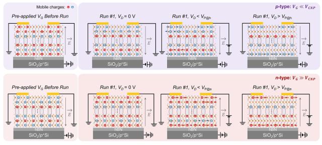
The key was the voltage the device had just experienced. When the researchers applied a control voltage of one polarity and then reversed it, the switch left behind a temporary imbalance in how electric charge was distributed inside the material. While that imbalance lasted, raising the operating voltage made the current fall instead of rise, the signature of NDR.
The team called the mechanism bias-history-driven, meaning the device's behavior depends on its recent electrical past.
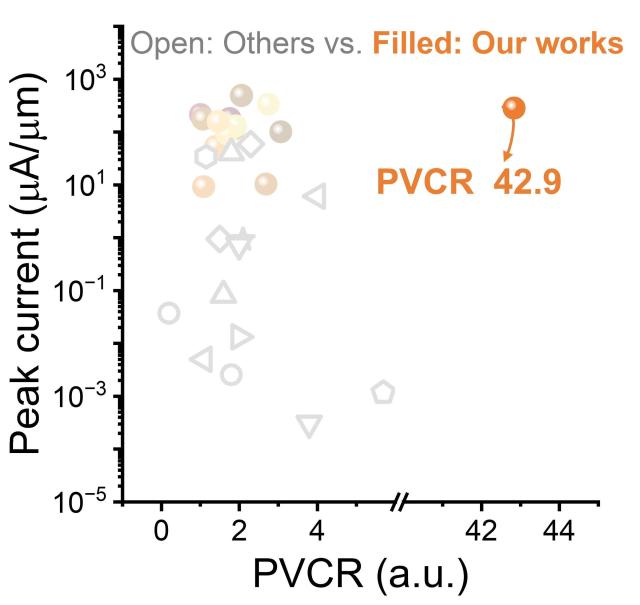
Performance reached practical territory. With its surface protected by a thin polymer coating, the device recorded a peak-to-valley current ratio of up to 42.9 at room temperature, a standard measure of how sharply the current drops during the NDR effect, along with a peak current of 280.8 microamperes per micrometer of channel width.
The researchers suspect the effect is connected to electrical polarization inside the layered material, but that link has not yet been demonstrated and is the subject of follow-up work.
Sim Eun-ji, a student in the Department of Applied Physics, was the first author of the paper, with students Seong Su-in and Jeong Yu-jeong also taking part. Ko Chang-hyun, a professor in the same department, joined the work, as did Alessandro Cresti and Christoforos Theodorou of the CROMA laboratory under France's National Center for Scientific Research (CNRS). The study was conducted jointly with Semi Otter Edu Corporation.
The findings were published in ACS Nano, a journal of the American Chemical Society.
The research was funded by the Ministry of Science and ICT and the National Research Foundation of Korea through the mid-career researcher program, the Korea-France PHC STAR international cooperation program jointly backed by the foundation and the French government, and the Seoul ANCHOR Center project supported by the Ministry of Education and the Seoul Metropolitan Government.
[Reference Information]
Journal/Source: ACS Nano (IF 17.3, JCR top 7.1%)
Title: Bias-History-Driven Negative Differential Resistance in Heterojunction-Free WSe2 Multilayers
Link/DOI: https://doi.org/10.1021/acsnano.6c15394

Park Sae-jin
Experienced journalist and editor at AJU PRESS specializing in multilingual news. I cover international diplomacy, geolpolitics, and policy, consistently delivering highly accurate, compelling reporting for a worldwide audience.
Copyright ⓒ Aju Press All rights reserved.