

SEOUL, November 16 (AJP) - The sprawling leadership debacle at Nvidia — often dubbed the AI central bank for its outsized influence over the global artificial intelligence ecosystem — has unsettled investors already questioning the durability of the AI spending boom.
Its Asian memory suppliers are nonetheless wasting no time expanding their factories to defend their technological lead against rising Chinese competition. Nvidia or not, the race for high-bandwidth memory (HBM) begins on the factory floor.
With demand outstripping available capacity, the challenge extends beyond developing faster chips. Manufacturers must build enough cleanroom space, secure increasingly complex equipment and demonstrate that new technologies can be produced reliably at commercial scale.
South Korea’s SK hynix brought that challenge into focus Monday with its Trinity Fab project, a dedicated testing facility inside its first semiconductor plant at the Yongin chip cluster, south of Seoul.
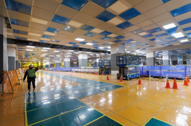
The 874.6 billion won ($655 million) project will allow domestic suppliers of semiconductor materials, components and equipment to test their products under conditions closely resembling a commercial production line. It addresses a bottleneck that can delay the adoption of new technologies for years.
The facility will house 55 pieces of equipment and systems, including 37 advanced production tools used in lithography, etching, deposition, cleaning and polishing. It is scheduled to open in May 2027, with full testing services beginning in the fourth quarter.
SK hynix is contributing 443.2 billion won, the central government 373.6 billion won and provincial and municipal authorities another 57.7 billion won.
The project aims to cut about one to one-and-a-half years from the time domestic suppliers need to move from product development to mass production, which currently averages three to four years.
An industry source familiar with the project told AJP that its main advantage was giving smaller suppliers access to manufacturing infrastructure they would struggle to establish independently.
“Smaller suppliers have difficulty creating their own cleanroom environments for semiconductor production,” the source said. “We’re providing them with the space so they can test their products under actual manufacturing conditions.”
The source added that SK hynix would help cover some initial research and development costs, including those associated with unsuccessful trials, to encourage suppliers to pursue more ambitious projects.
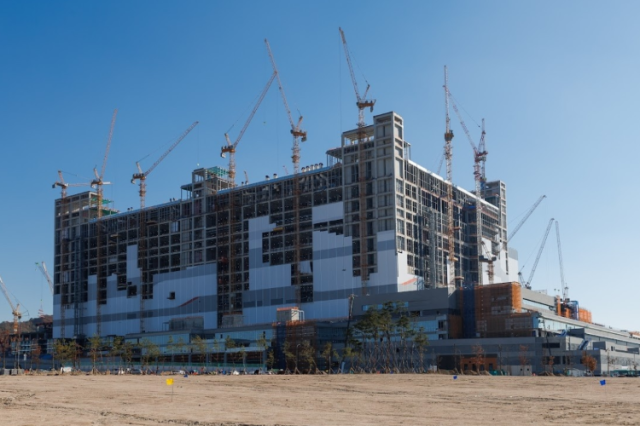
The testing facility occupies part of the company’s first Yongin fab, where construction is 89 percent complete. SK hynix plans to open the plant’s first cleanroom in February 2027 and begin commercial production in the fourth quarter.
The company has committed 600 trillion won to developing the broader Yongin semiconductor cluster as a major production base for advanced memory used in AI systems.
Trinity Fab addresses a fundamental manufacturing constraint: a material or machine that performs well in a laboratory may behave differently inside a commercial fab, where temperature, humidity, contamination and equipment configurations must be tightly controlled.
Even a small variation can reduce yields — the proportion of usable chips produced — making the transition from research to mass production costly and time-consuming.
Samsung Electronics is expanding its own manufacturing infrastructure at its Pyeongtaek campus, where construction of its fifth semiconductor production complex, P5, is underway.
The facility is expected to become a major production base for next-generation DRAM, including memory used in HBM, as Samsung builds capacity to meet demand from AI data centers.
Industry reports describe P5 as a three-story manufacturing complex that would accommodate more cleanroom space than Samsung’s existing two-story fabs, potentially increasing capacity within the same site.
Samsung has not publicly confirmed a detailed production timetable, although industry reports have pointed to operations beginning around 2028.
The expansion comes as Samsung prepares to raise output of its most advanced memory products.
During its third-quarter earnings conference call on Oct. 29, the company said it would begin mass production of HBM4E in the first half of 2027 and increase volumes in the second half. It also plans to expand sales of HBM4 and high-performance server DRAM.
Samsung expects memory supply to remain tight through 2028 as increasingly complex HBM designs require larger chips and more processing steps, constraining how quickly manufacturers can expand output.
The company projected total capital expenditure of 84.4 trillion won for 2026, including 76.8 trillion won for its semiconductor division. Investment in new fabs and infrastructure is intended to support AI-related demand.
Alongside factory construction, Samsung has built a supplier support system covering technology development, equipment access and production testing.
Since 2015, it has supplied more than 10,000 patterned wafers to domestic suppliers, research institutions and universities to help them evaluate materials and equipment, according to company data. Joint technology development projects with domestic suppliers rose from 76 in 2019 to 141 in 2025.
Samsung also provides manufacturing and research equipment to outside organizations, participates in the MoaFab shared manufacturing initiative and evaluates domestically developed materials and equipment on its commercial production lines.
It has invested approximately 800 billion won in 34 domestic semiconductor materials, components and equipment companies, alongside broader financial and technical support programs.
These initiatives span multiple facilities and programs. Whether P5 will include a dedicated supplier testing center comparable to Trinity Fab has not been confirmed.
The construction race extends beyond South Korea.
U.S. memory maker Micron Technology is building DRAM production facilities in Idaho and New York as it seeks to expand domestic manufacturing and strengthen its position in advanced memory.
Micron expects its first new Idaho fab to begin producing DRAM wafers in mid-2027, with a second targeting initial production in late 2028.
In New York, the company broke ground on its first planned manufacturing facility in January 2026 and completed its first foundation concrete pour in July. Initial wafer production is expected in 2030.
Micron has outlined plans to invest more than $250 billion in U.S. manufacturing and research through 2035, with a long-term goal of producing 40 percent of its DRAM domestically.
The timetable illustrates the long lead times involved: building a fab is followed by equipment installation, process qualification and the gradual increase to commercial output.
Taiwan Semiconductor Manufacturing Co. (TSMC), the world’s largest contract chipmaker, is pursuing a parallel expansion in advanced processors and packaging technologies used alongside HBM in AI accelerators.
Its first Arizona plant began high-volume production using 4-nanometer technology in late 2024. A second facility is targeting 3-nanometer mass production in the second half of 2027.
Additional facilities are under construction as TSMC expands its U.S. footprint, including capacity for 2-nanometer and more advanced technologies.
TSMC does not compete in HBM memory. It manufactures advanced logic chips for customers including Nvidia and AMD, placing its factories in another critical part of the AI semiconductor supply chain.
The companies’ investments serve different markets and production needs, but share a practical constraint: advanced chip designs have commercial value only when manufacturers can reproduce them consistently, in sufficient volumes and at viable yields.
Nvidia’s leadership turmoil has sharpened questions about the future of AI spending. The factories now taking shape reflect commitments extending well beyond that immediate uncertainty — and a competition increasingly determined by how quickly new technology can reach dependable mass production.

Candice Kim
Candice Kim is a dedicated business and technology reporter specializing in the intersection of high-tech innovation and fast-paced consumer trends. Her core beats span the semiconductor, IT, cosmetics, and retail sectors, where she provides in-depth coverage of industry titans including Samsung Electronics, SK hynix, and LG Electronics, alongside leading consumer brands like Olive Young and Musinsa. Whether analyzing complex silicon supply chains or tracking the latest shifts in beauty and fashion retail, Candice is committed to delivering sharp, accurate reporting that keeps readers informed on the forces shaping today's most dynamic markets.
Copyright ⓒ Aju Press All rights reserved.