
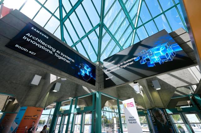
SEOUL, August 05 (AJP) - Samsung Electronics and SK hynix used the same stage at the Future of Memory and Storage (FMS) conference in Santa Clara this week to make two different arguments for who will shape artificial intelligence's next memory era, underscoring how South Korea's chip champions are now competing as much over future architecture as today's products.
The rivalry matters well beyond the two companies. Together, Samsung Electronics and SK hynix dominate the high-bandwidth memory (HBM) market that has become one of the AI industry's most closely watched supply chains, making their technology roadmaps a barometer for where AI infrastructure is heading next.
Samsung's keynote looked furthest ahead.
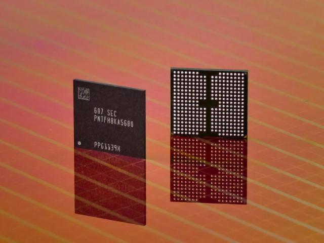
None of the technologies carries a commercialization timetable, underscoring Samsung's emphasis on defining the next generation of AI memory architecture rather than near-term product launches.
The broader roadmap nevertheless reinforced Samsung's ambition to remain an end-to-end AI memory supplier. The company highlighted HBM4E, HBM5, LPDDR5X-PIM and enterprise SSDs while stressing its position as an integrated device manufacturer spanning memory, foundry and advanced packaging.
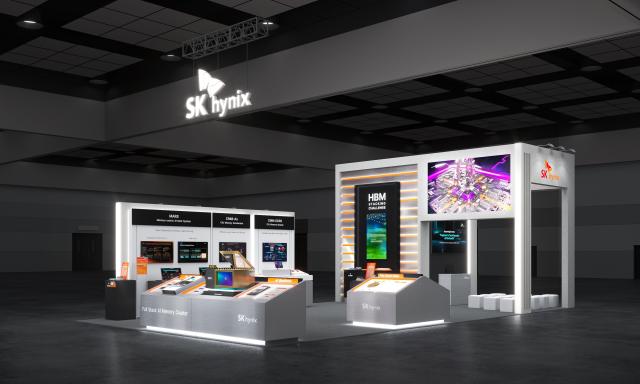
Published through the Open Compute Project (OCP) consortium, the specifications establish an open standard already backed by Google and AI chip startup Tenstorrent, aiming to accelerate adoption across GPU and CPU platforms. Rather than replacing HBM, HBF is designed to complement it by providing significantly larger memory capacity at far lower cost, addressing one of the biggest bottlenecks facing large-scale AI inference and agentic AI systems.
SK hynix also showcased its 375-layer V10 4D NAND, with mass production of enterprise SSDs based on the technology scheduled for early 2027, reinforcing its strategy of bringing next-generation storage products to market quickly.
Samsung focused on defining where AI system architecture could evolve beyond today's HBM, using concept technologies to position itself at the center of future memory design, whereas SK hynix concentrated on extending its leadership in commercial AI memory by advancing technologies already moving toward industry adoption through open standards and near-term production.
FMS is less a product launch event than a forum where semiconductor companies stake out technology roadmaps years before widespread deployment. Both companies choosing the same conference to unveil competing visions beyond conventional HBM signals an increasingly strategic contest over who will define the next phase of AI infrastructure after today's HBM boom.
Samsung's vision centers on vertically integrating memory and compute into increasingly three-dimensional architectures. SK hynix is betting the next bottleneck will be AI inference, requiring an entirely new tier of memory between HBM and storage. For now, the two companies are pursuing different routes toward the same goal: becoming the indispensable memory supplier for the AI industry's next decade.
AJP Takeaways:
— Samsung and SK hynix presented competing AI memory roadmaps at the Future of Memory and Storage (FMS) conference in Santa Clara, held the week of August 3-7, 2026.
— Samsung unveiled concept-stage technologies with no commercialization date: zHBM (memory stacked directly on AI accelerators, claimed up to 8x HBM5 performance), zNAND-O for edge AI, and V10 Bonding V-NAND, the first wafer-bonded NAND exceeding 400 layers.
— SK hynix and SanDisk published the industry's first open specifications for High Bandwidth Flash (HBF) through the Open Compute Project, backed by Google and Tenstorrent; HBF is designed to sit between HBM and SSDs for terabyte-scale AI inference workloads.
— SK hynix's 375-layer V10 4D NAND enterprise SSDs are scheduled for mass production in early 2027.
— The split reflects two strategies: Samsung is positioning itself around future 3D memory-compute architecture, while SK hynix is extending its lead in memory already moving toward open-standard, near-term commercial adoption.

Copyright ⓒ Aju Press All rights reserved.